Shared and Custom Silicon Nitride
Wafer Run
From shared MPW prototypes to fully custom wafer production.
Every wafer is built on our patented copper-free silicon platform and Photonic Damascene process, the same foundation behind our own microcomb modules. The result is an ultra-low-loss Si₃N₄ platform, available as shared MPW reticles or fully custom runs. We also provide monolithic integration of Sc-doped AlN piezoactuators.
From Substrate Innovation to Fabrication Access
Conventional silicon nitride platforms are constrained by thermal drift and unpredictable soliton formation.
Deeplight addresses this problem: we engineered the substrate and process to eliminate the physics problem at its source. Our patented copper-free wafers and Photonic Damascene process deliver ultra-low loss and ultra-low thermal absorption — enabling deterministic soliton generation with simple laser tuning.
We offer both shared MPW and fully dedicated wafer runs for research, prototyping, and production.
Key Features
Ultra-low thermal absorption
Proprietary copper-free Silicon wafers eliminate parasitic heating, improving soliton stability.
Thick Si₃N₄ films (> 800 nm)
High anomalous dispersion and strong Kerr nonlinearity for broadband comb initiation.
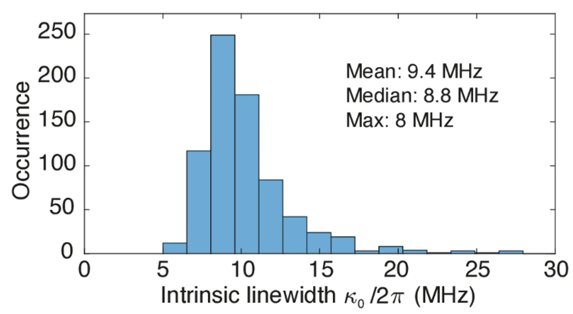
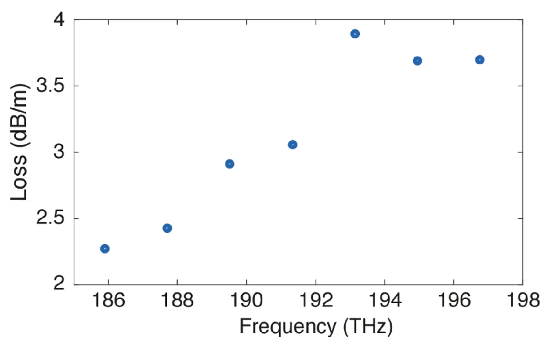
Ultra-low Propagation loss (< 3 dB/m)
Enabled by our proprietary Photonic Damascene process, delivering the high-Q micro-resonators required for stable soliton generation.
Full design support included
From DRC-verified layout and simulation to experimentally-tested components, everything you need to go from concept to a foundry-ready design
Monolithic Integration of Piezo actuators and micro-heaters
Add active tuning to your photonic chip. Piezo actuators deliver high-linearity, low-power mechanical control, while integrated micro-heaters handle thermal tuning
Custom and shared runs available
flexible options from academic R&D prototyping through to volume production.
Fabrication Run Options
| Shared MPW Run | Custom Wafer Run | |
|---|---|---|
| Best For | R&D prototyping, academic research, proof-of-concept | Volume production, proprietary designs, full-wafer control |
| Cost Model | Shared wafer cost across multiple users | Dedicated wafer pricing |
| Design Flexibility | Standard reticle allocation | Full reticle customization |
| Turnaround | Scheduled run calendar | Priority scheduling available |
| SiN Thickness & Wafer size | 200 nm & 900 nm, 4 inch | Custom thickness available, 4 inch |
| Add-ons | Micro-heaters, Piezo actuators, DRC check | Micro-heaters, Piezo actuators, DRC, packaging support |