
Silicon Nitride Photonics
Fabrication Run
Your silicon nitride photonics designs fabricated on the copper-free silicon nitride platform behind our own products.
Research groups and development teams that need a chip beyond our catalogue get the same substrate, the same photonic Damascene process developed at EPFL and licensed to Deeplight, and the same building blocks we use ourselves: copper-free silicon wafers, thick Si₃N₄ resonators, monolithic Sc doped-AlN piezo actuators and micro-heaters. A device that works in a Deeplight run is already a Deeplight device, one step from a product or from partner manufacturing.
Deeplight is not a general-purpose PIC foundry and may decline designs outside this scope.
From Substrate Innovation to Fabrication Access
A soliton microcomb is only as stable as the substrate underneath it.
Absorption in the substrate heats the resonator and drifts it in the very moment the soliton forms. Deeplight's copper-free silicon substrate and photonic Damascene process remove that absorption at its source. That is why single solitons on our platform are reached deterministically with simple laser tuning, in our products and in your devices.
Start with a shared-reticle device run for your first devices and design iterations, or take a dedicated wafer run when you need the full wafer for your own variants.
Key Features
Ultra-low thermal absorption
Proprietary copper-free Silicon wafers eliminate parasitic heating, improving soliton stability.
Thick Si₃N₄ films (> 800 nm)
High anomalous dispersion and strong Kerr nonlinearity for broadband comb initiation.
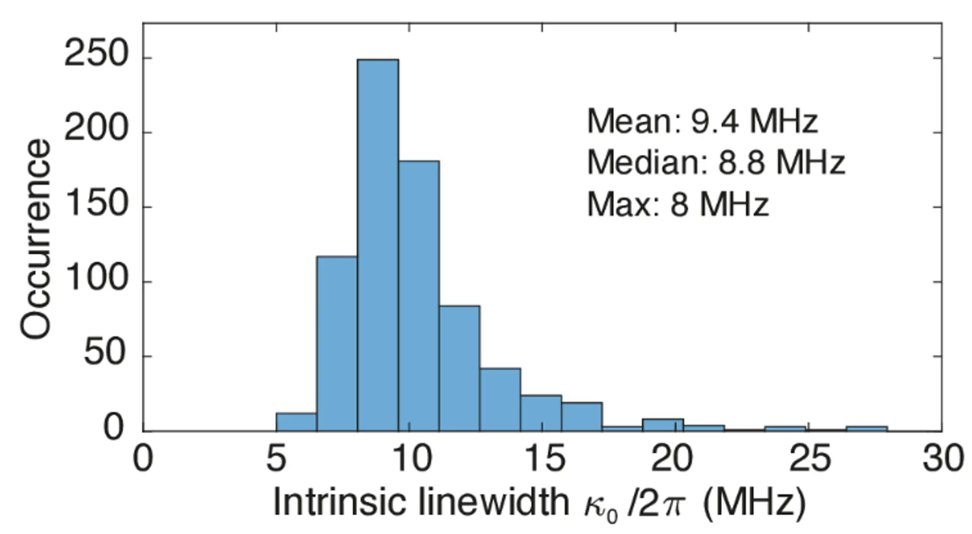
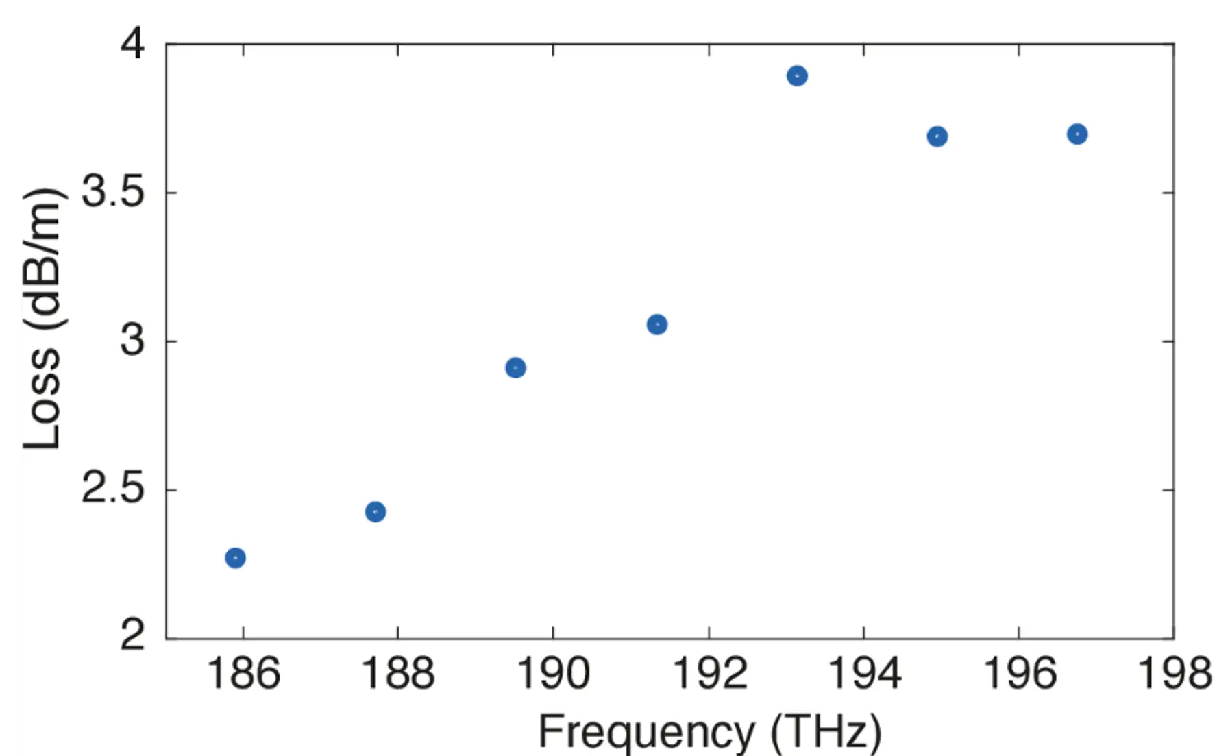
Ultra-low Propagation loss (< 3 dB/m)
Enabled by our proprietary Photonic Damascene process, delivering the high-Q micro-resonators required for stable soliton generation.
Design support included
Dispersion and coupling design, DRC-verified layout and tested resonator and actuator building blocks, from the engineers who design our own microcomb modules and lasers.
Monolithic Integration of Piezo actuators and micro-heaters
Add active tuning to your photonic chip. Piezo actuators deliver high-linearity, low-power mechanical control, while integrated micro-heaters handle thermal tuning
Shared-reticle and dedicated runs available
flexible options from academic R&D prototyping through to dedicated wafer runs for proprietary designs.
Fabrication Run Options
| Shared-reticle device run | Dedicated wafer run | |
|---|---|---|
| Best For | First devices and design iterations: research groups and development teams building soliton microcombs, Kerr combs, linear and nonlinear waveguides | Your own variants on your own wafer: pilot quantities and proprietary designs |
| Cost Model | Shared wafer cost across multiple users | Dedicated wafer pricing |
| Design Flexibility | Standard reticle allocation | Full reticle customization |
| Turnaround | Scheduled run calendar | Priority scheduling available |
| SiN Thickness & Wafer size | 200 nm & 900 nm, 4 inch | Custom thickness available, 4 inch |
| Add-ons | Micro-heaters, Piezo actuators, DRC check | Micro-heaters, Piezo actuators, DRC, packaging support |
Upcoming Scheduled Run Calendar
Shared-reticle device run 2026-Q4
Design submission deadline: 1 November 2026
Shared-reticle device run 2027-Q2
Design submission deadline: 1 April 2027